
 English
Views: 0 Author: Site Editor Publish Time: 2026-08-13 Origin: Site


You define a transistor as a three-terminal semiconductor device that switches or boosts electronic signals. You control current flow across terminals to run modern electronic circuits in many different uses. Circuit designers group these parts into two main transistor types based on how they work. You use current-driven bipolar junction transistors to get high signal boosting in specific setups. A classic bjt uses both electron and hole paths to carry current. On the other hand, you use voltage-driven field-effect transistors to reduce input power loss. Understanding each transistor helps you pick the best parts for smooth switching performance. Every solid-state transistor works using exact electric field or charge injection methods.
Circuit designers use two main transistor types: current-driven bipolar transistors and voltage-driven field-effect transistors.
NPN transistors switch faster than PNP transistors because electrons move quicker than holes inside semiconductors.
Transistors work just like open or closed light switches, depending on their current settings and electrical power.
New silicon carbide and gallium nitride materials boost energy efficiency in high-power electronic devices.
Inside every semiconductor device, free charge carriers move through the crystal lattice when you apply voltage. Electrons and holes move at different speeds under identical electric fields. You calculate electron drift speed with vd = mu_e x E, where mu_e represents electron mobility. You calculate hole drift speed with vd = mu_h x E, using hole mobility mu_h.
Carrier Type | Effective Mass (m0) | Mobility at Room Temperature (cm²/V·s) |
|---|---|---|
Electron | 0.26 | ~1,350 |
Hole | 0.39 | ~480 |
Electrons move faster than holes because they possess lower effective mass. This mobility difference changes how you design an active transistor circuit for high-speed operation. NPN configurations pass current faster than PNP configurations due to superior electron movement.
External bias voltages control junction barrier width and drive carrier injection across the PN boundary. The base-emitter voltage directly dictates the collector current inside a bipolar transistor. Heat alters this electrical relationship during continuous operation.
Temperature Rise: Surroundings warm up or power usage boosts internal junction heat.
Current Escalation: Collector current jumps because the base-emitter junction responds strongly to heat.
Heat Generation: Power loss grows according to P = V x I, creating extra thermal energy.
Thermal Runaway Loop: Ongoing self-heating loop causes permanent device failure unless protective circuits stop it.
Base-emitter voltage drops by approximately -2 mV/°C as junction temperature rises under constant current. The collector current equation IC = IS x e^(VBE/VT) uses thermal voltage VT, which equals approximately 26 mV at room temperature. Fixed bias circuits can double their current every 5 to 10 °C without thermal compensation. You prevent component damage by adding an emitter resistor, which creates self-stabilizing feedback. Designers must apply these fundamental operating principles to maintain target bias points across all standard working conditions.
People group main transistor types by their internal structure and carrier motion. You make an npn transistor by putting P-type material between two N-type parts. You build a pnp device by putting N-type material between two P-type parts. Electric current moves through these bipolar devices using electrons and positive holes.
NPN transistors usually switch faster than PNP transistors. This happens because electrons move quicker in NPN units than holes do in PNP units.
Since electrons travel faster than holes, an npn device turns on much quicker. You control a classic bjt device by sending steady current to its base. The base pin needs this constant flow to keep charges moving across layers.
You use field-effect transistors to manage output current by using gate voltage rather than current flow.
Characteristic | Bipolar Junction Transistors (BJTs) | Field-Effect Transistors (FETs) |
|---|---|---|
Control Mechanism | Driven by small input base current | Driven by gate voltage creating electric field |
Charge Carriers | Bipolar (uses electrons and holes) | Unipolar (uses single carrier type in channel) |
Input Impedance | Moderate (several kilohms) | High (infinite DC impedance from gate oxide) |
Input Current Flow | Requires continuous base current | Negligible gate current under DC conditions |
A power mosfet has high input impedance because a thin gate layer blocks current. You put voltage on the gate pin to create an electric field inside. Fast action in a power mosfet relies on gate charge during state changes.
During turn-on, incoming gate current fills device capacitance through the Miller phase. Drain voltage falls while gate voltage stays the same during this short time. You reduce power loss in a circuit by sending enough current to clear gate charge.
You shift a bjt across three distinct states to control modern solid-state circuits. Both internal junctions stay reverse-biased while the component remains in cut-off mode. Base voltage sits below emitter and collector potentials, keeping base-emitter voltage under the 0.6V threshold. This halts carrier movement, making the transistor act just like an open switch.
Operating Mode | Junction Bias Status | Pin Voltage Conditions (NPN) | Critical Voltage Thresholds |
|---|---|---|---|
Cut-off Mode | Both junctions reverse biased | V_B < V_E and V_B < V_C | V_BE < V_th (~0.6V) |
Active Mode | Base-Emitter forward biased; Base-Collector reverse biased | V_E < V_B < V_C | V_BE >= V_th (~0.6V) |
Saturation Mode | Both junctions forward biased | V_B > V_E and V_B > V_C | V_BE > V_th; V_CE reaches 0.05V - 0.2V |
Active mode requires a forward-biased base-emitter boundary along with a reverse-biased base-collector boundary. For npn parts, you place base voltage between the emitter and collector values. Supplying at least 0.6V to the base-emitter junction creates steady signal amplification. A pnp setup instead needs base voltage kept lower than the emitter voltage. Forward-biasing both junctions forces the component straight into saturation mode. Your npn part conducts fully as a closed switch, dropping collector-to-emitter voltage to 0.05V–0.2V.
Adjusting gate voltage allows you to control total power flow inside a mosfet. A conductive channel starts forming once gate-to-source voltage reaches the threshold limit.
Sending positive gate voltage pulls free electrons over to balance out substrate ions.
Collecting enough electrons finishes surface inversion and builds the conductive channel path.
Raising gate voltage above threshold pulls in extra electrons, widening the channel for current.
Your mosfet works in the linear region while drain voltage remains below gate voltage minus threshold voltage. Output current increases smoothly alongside drain voltage across this open path. Raising drain voltage until it matches gate voltage minus threshold voltage causes channel pinch-off. Past this limit, the inverted channel shrinks right near the drain edge. Extra voltage pushes the transistor into saturation, where current settles into a constant flow.
Specific circuit layouts help process weak signals while keeping them clear and strong. Engineers choose different bjt pin setups to balance input resistance with overall voltage amplification. Your design depends on the input source resistance alongside the required output load needs. These small-signal networks reliably handle sensor data while maintaining clear signals through every stage.
Every layout option offers special advantages for radio frequency and audio communication setups. You compare common emitter, common collector, and common base circuits to balance signal levels.
Configuration | Input Impedance | Voltage Gain |
|---|---|---|
Common Emitter (CE) | Low (~50 kΩ) | High (~500) |
Common Collector (CC) | Very High (~750 kΩ) | Less than unity (< 1) |
Common Base (CB) | Very Low (~40 Ω) | Moderate/Small (~150) |
Power circuits need fast switching during pulse-width modulation to prevent wasted energy losses. Fast gate drivers quickly push electrical charge into your mosfet during power state changes. High-current drivers work with small series resistors to fine-tune exact switching speeds. Placing a Schottky diode across the gate resistor speeds up shutoff while managing startup across main transistor types.
Motors and relays send high voltage spikes back through circuits during sudden shutoff events. A simple freewheeling diode protects your switching transistor by catching these dangerous power spikes safely.
Catches the reverse voltage created when a magnetic coil turns off and collapses.
Stays blocked during normal use, but opens up when a power spike appears.
Routes extra current safely through a loop to protect the drive transistor from damage.
These protective circuits keep industrial equipment working safely while extending component lifespans in setups using a secondary bjt power stage.
Engineers choose each electronic component by carefully checking data sheets before building new projects. Checking maximum drain-to-source voltage VDS prevents dangerous electrical breakdown. Reviewing on-state resistance RDS(on) stops excess power dissipation in a power mosfet. Lower internal resistance helps an active circuit run much cooler. Calculating thermal resistance RthJC measures how heat moves from junction to case.
Good heat management protects sensitive parts from lasting component damage. Every switching transistor handles heat through attached metal heat sinks. These parts draw extra heat away from the working chip. Dongguan Merry Electronic Co., Ltd, known as MeiZhao Electronic, produces high-reliability transistor models for tough settings. This trusted semiconductor supplier maintains ISO9001, ISO14001, and IATF16949 quality certifications. Their team creates durable power setups for cars, factory tools, and power systems.
New technology uses wide bandgap materials like Silicon Carbide (SiC) and Gallium Nitride (GaN). These modern choices work better than older silicon parts in high-voltage designs. Fast electron movement helps a wide bandgap transistor switch faster. Better heat resistance means circuits need less bulky cooling equipment.
Parameter / Feature | Legacy Silicon (Si) | Silicon Carbide (SiC) | Gallium Nitride (GaN) | Key Advantage Driven by Wide Bandgap |
|---|---|---|---|---|
Bandgap Energy | 1.1 eV | 3.3 eV | 3.4 eV | Allows operation at higher temperatures, voltages, and frequencies. |
Breakdown Field Strength | 0.3 MV/cm | 3.5 MV/cm | 3.3 MV/cm | Nearly 10x higher strength handles higher operating voltages. |
Max Operating Temperature | 150°C | Up to 200°C | Up to 200°C | Enables stable operation in high-heat environments. |
Electron Mobility | N/A | 650 cm²/Vs | 2,000 cm²/Vs | Enables up to 10x faster switching speeds and frequencies. |
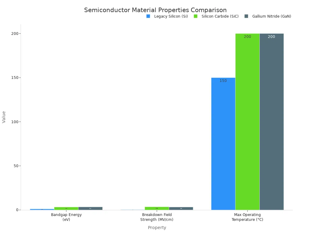
Circuits save more energy when upgraded to advanced SiC and GaN options. These parts lower energy waste in large electrical systems. MeiZhao Electronic serves as a major semiconductor supplier offering new SiC devices and power transistor units for modern high-power setups.
Picking the right transistor depends on how you power it. A bjt needs continuous base current to work. This steady flow generates extra heat in your circuit. On the other hand, field-effect transistors rely on gate voltage. That simple voltage control cuts down input power loss.
You must balance working principles with heat limits when designing circuits. Keeping things within safe bounds protects every semiconductor device from heat damage.
New SiC and GaN materials provide much higher efficiency for modern tech. Running a wide-bandgap mosfet inside safe limits prevents threshold voltage drift. You can build faster, cooler projects by picking the right transistor for your system.
You choose between two main transistor types: current-driven bipolar junction devices and voltage-driven field-effect devices. Each choice handles power differently to fit your project.
An npn device moves current using fast electrons. A pnp device relies on slower positive holes. You get faster switching speeds when you pick npn parts for active circuit boards.
You use a solid-state transistor to boost signals or turn big currents on and off. Common uses include car power units, factory machines, home gadgets, and phone networks.
You check voltage breakdown limits and internal heat resistance on data sheets. You can choose high-efficiency SiC devices from MeiZhao Electronic to lower power loss in hot settings.


