
 English
Views: 0 Author: Site Editor Publish Time: 2026-10-16 Origin: Site


Have you ever wondered how a tiny sensor signal can run a big motor? The answer is an NPN transistor. The npn transistor is a part with three terminals. It switches and boosts electronic signals. Two N-type layers sit around a P-type layer. The three terminals are the Emitter, Base, and Collector. This npn transistor is a key building block. You see npn transistors in simple LED circuits and complex microprocessors. This part powers everything from toys to computers. This post covers the npn symbol, how it works, and three main uses. Knowing this transistor helps you understand many electronic devices.
An NPN transistor has three terminals: the emitter, the base, and the collector.
The symbol shows an arrow on the emitter that points outward.
A small current at the base controls a bigger current in the collector.
Use an NPN transistor as a switch to turn loads on or off.
Amplifiers make weak signals stronger by using the transistor's active region.
Logic gates use transistors that are either fully off or fully on to handle digital signals.
Check the datasheet for its voltage, current, and gain ratings.
Pick a trustworthy supplier to get good transistors.
Every circuit diagram uses a standard symbol to represent an npn transistor. This symbol acts as a visual shorthand. It tells you exactly how the component connects to other parts. The symbol shows three terminals: the base, the collector, and the emitter. Each terminal has a distinct line and position. You will see this symbol in countless schematics, from simple hobby projects to professional industrial designs.
The schematic symbol for an npn transistor looks like a simple diagram. A vertical line represents the base. A diagonal line meets the base at an angle, representing the collector. Another diagonal line meets the base on the opposite side, representing the emitter. The collector line and the emitter line do not connect to each other directly. They both connect to the base line. This visual separation reminds you that the base region sits between the collector and emitter regions inside the actual device.
Look closely at the emitter line. You will notice a small arrowhead on it. This arrow is not decorative. It carries critical information about the transistor type. For an npn transistor, the arrow always points outward, away from the base. This outward arrow indicates the direction of conventional current flow. Current flows from the collector, through the transistor, and out of the emitter. The arrow direction tells you that this device works best for low-side switching applications. In these circuits, the load connects between the positive supply and the collector, while the emitter connects to ground.
The pnp transistor symbol looks almost identical at first glance. The only difference lies in the emitter arrow direction. For a pnp transistor, the arrow points inward, toward the base. This small change signals a completely different current behavior. The arrow direction also tells you about the switching application. NPN transistors suit low-side switching, where the load sits above the transistor. PNP transistors suit high-side switching, where the load sits below the transistor. Remember that the arrow represents semiconductor physics, not the physical orientation of the package. You cannot determine which physical pin is which just by looking at the symbol.
The schematic symbol does not tell you the physical layout. Real npn transistors come in various packages. Each package has a different pin arrangement. You must always check the datasheet for the specific part number. The pinout varies with the package type and the manufacturer. Guessing the pinout can damage your circuit or the transistor itself.
The TO-92 package is a small, plastic, three-lead package. It handles low power signals. You will find this package in many general-purpose npn transistors. The pinout depends on the series. For JEDEC 2N series parts like the 2N3904, the pins are Emitter, Base, Collector from left to right when you look at the flat face. For Pro Electron BC series parts like the BC547 or BC548, the pins are Collector, Base, Emitter. Japanese 2S series parts use yet another arrangement: Emitter, Collector, Base. Always verify the pinout before you solder.
The TO-220 package handles much higher currents and power levels. This package has a metal tab that helps dissipate heat. The tab often connects to the collector internally. For example, the TIP31C and TIP41C npn transistors use a Base, Collector, Emitter pinout. The metal tab serves as the collector connection. You may need to insulate the tab from the heatsink in some circuits. Always consult the datasheet to confirm the exact pin functions for your chosen part.
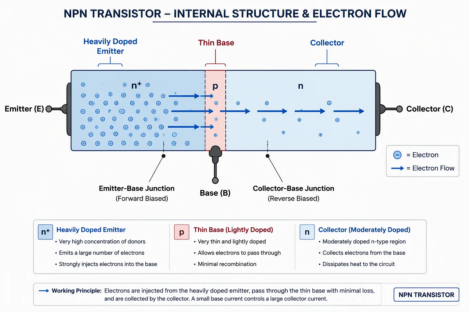
To understand how an npn transistor works, you must look inside it. You need to see how its three parts interact. The key action happens where these parts meet. This section covers the internal build, the bias conditions, and the current flow that make npn transistors so helpful.
The npn transistor build creates two PN junctions inside one crystal. The emitter-base junction sits between the emitter and the base. The collector-base junction sits between the collector and the base. These two junctions share the thin base area. Their behavior controls everything the transistor does.
The emitter area holds a very high amount of n-type impurities. Engineers call this "heavy doping." This heavy doping has a key job. It provides a huge number of free electrons for the base. Think of the emitter as a tank full of charge carriers. When you forward-bias the emitter-base junction, these electrons rush into the base area.
The base area lies between the emitter and collector. It is very thin, often under one micrometer wide. The base also has a light amount of p-type impurities. This light doping matters for two reasons. First, it keeps base resistance low enough for control signals to work. Second, it lowers the chance that electrons recombine with holes while crossing the base.
The doping imbalance between areas is planned. The heavily doped emitter sends electrons well, while the lightly doped base stops hole injection from the base side. This balance makes sure electron flow leads the transistor's operation.
The collector area uses moderate n-type doping. It does not need to send carriers. Instead, it gathers the electrons that make it across the base. The collector area is physically bigger than the emitter. This bigger size helps remove heat and handle higher voltages. The collector-base junction also has a wider depletion area than the emitter-base junction. This wider depletion area gives the transistor its voltage-handling ability.
Biasing means applying outside voltages to the transistor terminals. These voltages set the working conditions. For an npn transistor to boost signals, you must bias it right. The wrong bias pushes the transistor into an unwanted mode.
You must forward-bias the base-emitter junction. This means connecting the base positive compared to the emitter. For a silicon npn transistor, the base-emitter voltage must hit about 0.7 volts. This voltage matches one diode drop because the base-emitter junction acts like a forward-biased diode.
For a silicon NPN transistor, the base-emitter voltage drop (Vbe) is about 0.7 V—equal to one diode drop—and the base voltage must go above this value for the transistor to conduct.
When you apply this forward bias, the junction's depletion area narrows. Electrons from the emitter gain enough energy to move into the base. This forward bias condition starts the current flow process.
You must reverse-bias the base-collector junction. This means connecting the collector positive compared to the base. The reverse bias widens the depletion area at this junction. This widened area creates a strong electric field. That field pulls electrons from the base into the collector. Without this reverse bias, the transistor cannot work as an amplifier.
When both junctions have the right bias, the transistor enters its active region. In the active region, the transistor can boost signals evenly. The current flow follows a steady pattern. Knowing this pattern helps you build circuits with confidence.
Picture a water valve in a pipe. A small handle turn controls a large water flow. The npn transistor works the same way. A small base current acts like the handle. It controls a much larger collector current. You turn the base current up or down. The collector current follows in step. This analogy captures the core of transistor action. A tiny input signal manages a large output current.
The currents in a transistor follow a simple rule. The emitter current equals the base current plus the collector current. You can write this as IE = IB + IC. The emitter current is always the biggest. The base current is always the smallest. This rule holds true in every working region.
The process follows a sequence: injection, diffusion transport, and collection. Electrons inject from the heavily doped emitter into the base. They spread across the thin base due to a concentration difference. Most electrons reach the collector-base junction. The reverse-biased junction's field pulls them into the collector. Only a small number of electrons recombine with holes in the base. That small number becomes the base current.
The transistor's boosting power comes from current gain. Engineers define this gain as hFE = IC / IB. The collector current divided by the base current gives you the gain value. Typical small-signal transistors have hFE values between 100 and 300. This means a base current of 1 milliampere can control a collector current of 100 to 300 milliamperes.
The DC current gain is defined as hFE = IC / IB. In the active region, the parts of carriers lost by recombination and gathered by the collector stay proportional as the injected carrier amount changes. This proportionality explains why a small base current controls a larger collector current.
The active region operation depends on this proportional link. When you run the transistor in the active region, the collector current becomes a direct copy of the base current, scaled by the gain factor. This direct link forms the base for amplifier circuits. The transistor does not create energy. It moves energy from the collector supply to the output load. The small base signal only guides this move.
Effect on depletion regions: The doping level sets the depletion region width. A lightly doped area like the collector has a wider depletion region than a heavily doped one like the emitter. This explains why the collector-base junction has a wider depletion region than the emitter-base junction.
Effect on base transport: Because the base is very thin and lightly doped, only a few electrons recombine with holes in the base. This low recombination rate makes sure most injected electrons from the emitter reach the collector, supporting the transistor's current boosting function.
Knowing these ideas lets you predict how any npn transistor will act in your circuit. You can calculate the expected currents and pick proper resistor values. You can also spot when a transistor works outside its intended region. This knowledge turns you from a passive watcher into an active circuit builder.
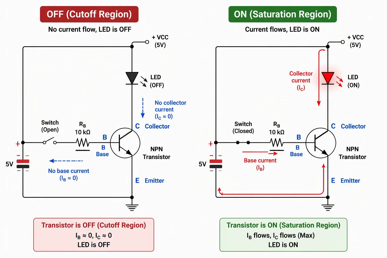
You can use an npn transistor as a simple switch. This mode does not use gradual amplification. Instead, the transistor operates in one of two states: fully OFF or fully ON. Think of a light switch on your wall. It has two positions, not something in between. An npn transistor works the same way in this application. You control the switch with a small current at the base. This small current then controls a much larger current through the collector.
Every npn transistor has three operating regions. For switching, you care about two of them: cutoff and saturation. These two regions correspond to the OFF and ON states of your switch. Understanding these regions helps you design reliable circuits.
The cutoff region represents the OFF state. In this condition, the transistor blocks current flow. No current passes from the collector to the emitter. For an npn transistor to reach cutoff, you must apply specific voltages. The voltage condition for cutoff is Vc > Vb < Ve. This means the collector voltage stays higher than the base voltage, while the base voltage stays lower than the emitter voltage. When you meet this condition, the base-emitter junction has no forward bias. Without forward bias, no electrons flow from the emitter into the base. The transistor acts like an open switch. No current flows through the load connected to the collector.
The saturation region represents the ON state. In this condition, the transistor conducts current fully. The voltage condition for saturation is Ve < Vb > Vc. Here, the base voltage rises above both the emitter and collector voltages. When you drive the transistor into saturation, the collector-emitter voltage drops to a very low value. For a typical silicon npn transistor, this saturation voltage (VCE(sat)) sits around 0.2V. Germanium transistors achieve a lower value near 0.1V. This low voltage means the transistor acts like a closed switch. Almost the entire supply voltage appears across your load.
Transistor Type | Typical VCE(sat) |
|---|---|
Silicon (common NPN) | 0.2V |
Germanium | 0.1V |
You can build a simple switching circuit with an npn transistor and an LED. This circuit demonstrates the switching concept clearly. You connect the LED and a current-limiting resistor between the positive supply and the collector. The emitter connects directly to ground. A base resistor connects between your control signal and the base terminal.
The base resistor serves a critical safety function. It limits the current flowing into the base. Without this resistor, the base would draw excessive current. This excessive current could damage both the transistor and your control circuit. The base-emitter junction acts like a diode. Once you apply about 0.7V across it, the current rises rapidly. The base resistor controls this current to a safe level.
You need to calculate two resistor values for this circuit. First, determine the base resistor value. You want enough base current to drive the transistor into saturation. A common rule uses a base current about one-tenth of the collector current. This ratio ensures the transistor saturates fully. Second, calculate the collector resistor value. This resistor limits the LED current to a safe operating level. Most standard LEDs operate well at currents between 10 and 20 milliamperes.
You can use the same switching principle to control larger loads. A relay or a DC motor requires more current than a microcontroller pin can supply. An npn transistor bridges this gap. This configuration is called a low-side switch. The load connects between the positive supply and the collector. The emitter connects to ground. When you apply a high signal to the base, the transistor turns ON. Current flows through the load, through the collector, and out the emitter to ground.
Consider the 2N2222 npn transistor. This popular part handles collector currents up to 800 mA. This rating applies to switching applications as well. You can control a small DC motor or a relay coil within this current limit. The relay coil might draw 100 mA. The motor might draw 500 mA. Both fall safely within the 2N2222's capability. For larger loads, you would select a power transistor with a higher current rating.
When you switch a relay or motor, you must consider inductive kickback. These loads store energy in their magnetic fields. When you turn OFF the transistor, this energy releases suddenly. This release creates a voltage spike that could damage the transistor. You should place a flyback diode across the load. This diode provides a safe path for the inductive current when the transistor switches OFF.
The switching circuit forms the foundation of digital electronics. Every logic gate, every microcontroller output, and every power management system relies on this principle. You can use npn transistors to interface between low-power control signals and high-power loads. This capability makes the npn transistor an essential tool in your electronics workbench.
Switching only turns things on or off, but amplification makes weak signals stronger. This ability makes the npn transistor a very flexible part. You use this mode when you need to boost a faint audio signal from a microphone or a sensor before sending it to a speaker or a recorder.
Amplification means taking a small input signal and creating a larger output signal that keeps the same shape. The npn transistor does this by working in its active region. In this region, the base-emitter junction gets forward-biased, and the base-collector junction gets reverse-biased. This setup lets a small base current control a much larger collector current in a steady ratio.
The active region lies between cutoff and saturation. Here, the collector current follows the base current in a straight line, scaled by the transistor's current gain (beta, β). This steady ratio keeps the input waveform intact while making it larger. The output stays a true, bigger copy of the input. Working in the active region needs careful biasing. You must set the DC voltages correctly so the transistor stays in this linear zone during the whole signal swing.
The common-emitter setup is the most used amplifier design. In this circuit, the emitter connects to ground through a resistor. The input signal enters through the base, and you take the output from the collector. This setup gives both voltage and current gain. The voltage gain formula is Av = -RL / (RE + r'e), where RL is the collector resistor, RE is the external emitter resistor, and r'e is the internal emitter resistance. The negative sign shows that the output flips the input signal. Higher voltage and power gains usually come from common-emitter operation compared to other setups.
You can build a single-stage audio preamplifier with a 2N3904 npn transistor. This circuit boosts a weak audio signal to a useful level. A typical design runs from a 9V supply with a collector current around 1 mA. The collector voltage sits at about 4.5V, roughly half the supply voltage, giving maximum signal swing.
Coupling capacitors play a key role in amplifier circuits. They block DC bias voltages from earlier or later stages while letting the AC audio signal pass through. An input coupling capacitor of 1 µF connects your audio source to the base. This capacitor stops the source's DC level from upsetting your carefully set bias point. An output coupling capacitor also isolates the next stage from your DC bias.
You set the DC bias point using a voltage divider network. Two resistors form this divider: a top resistor of 73 kΩ and a bottom resistor of 17 kΩ. This divider sets the base voltage at the right level. The collector resistor (4.5 kΩ) and emitter resistor (1 kΩ) finish the biasing network. An emitter bypass capacitor of 10 µF shorts the emitter resistor at audio frequencies, raising the gain. An emitter series resistor of 30–80 Ω lets you fine-tune the gain. This circuit gives a voltage gain of about -50 (50 times) across a bandwidth of 100 Hz to 100 kHz.
Think of a dynamic microphone producing a signal of only a few millivolts. This signal is too weak for a speaker or a recording input. Your preamplifier circuit boosts this signal to a useful level. The microphone connects through the input coupling capacitor to the base. The transistor amplifies the signal in its active region. The output appears across the collector resistor, ready for the next stage.
The input impedance of this circuit sits around 15 kΩ, which matches well with many dynamic microphones. The load impedance should be a few kΩ for best performance. This simple preamplifier shows how one npn transistor can turn a whisper into a clear, audible signal. You can use this same idea to amplify signals from guitar pickups, sensors, or any weak audio source.
You can build whole digital systems using npn transistors as switches. The trick is to run each transistor in only two states: fully OFF or fully ON. These states match the cutoff and saturation regions you learned about earlier. When you push a transistor into cutoff, it stops current completely. When you push it into saturation, it lets current flow fully. These two states line up perfectly with the binary world of ones and zeros.
Digital circuits use a simple language. They use two voltage levels to show information. A HIGH voltage means logic 1. A LOW voltage means logic 0. The npn transistor turns these voltage levels into choices about current flow. You send a HIGH signal to the base. The transistor turns ON. You send a LOW signal. The transistor turns OFF. This clean on-off behavior forms the core of every digital computer.
Engineers set exact voltage limits for logic levels. These limits make sure digital devices can talk to each other reliably. The standard comes from TTL (Transistor-Transistor Logic) families. You need to know four key thresholds:
Parameter | Voltage Level | Definition |
|---|---|---|
VOH (Output HIGH) | ≥ 2.7 V | Lowest voltage a TTL device gives for a HIGH signal |
VIH (Input HIGH) | ≥ 2.0 V | Lowest voltage needed at an input to be read as HIGH |
VOL (Output LOW) | ≤ 0.4 V | Highest voltage a TTL device gives for a LOW signal |
VIL (Input LOW) | ≤ 0.8 V | Highest voltage allowed at an input to be read as LOW |
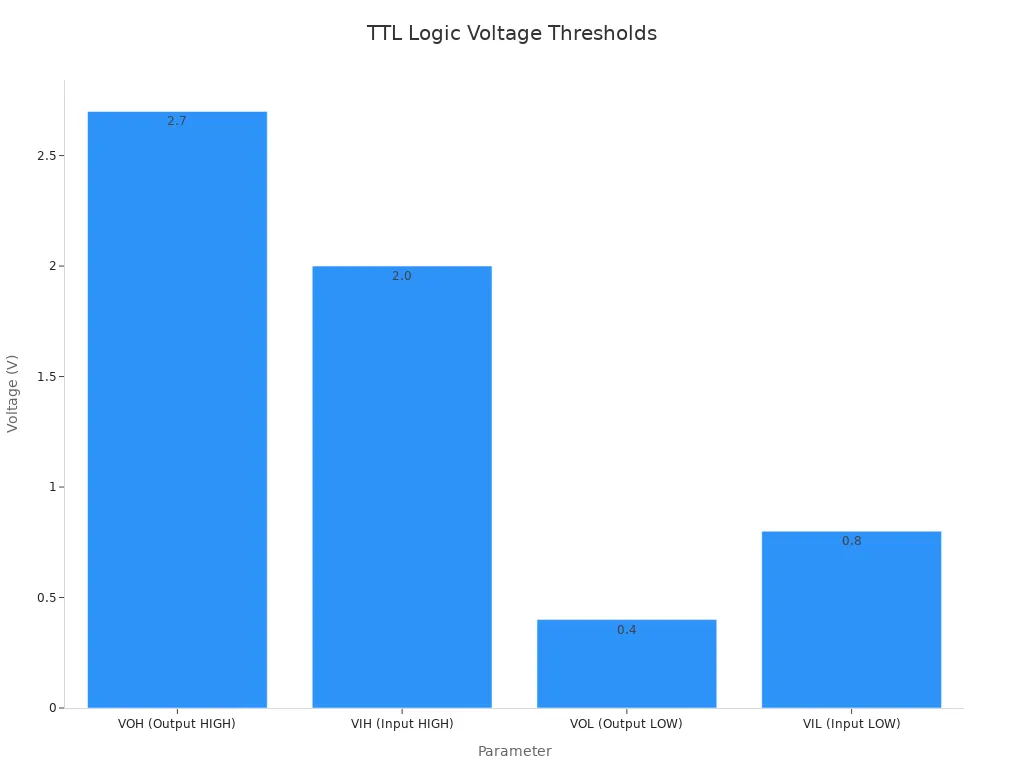
Notice the gap between 0.8 V and 2.0 V. This unclear zone gives unpredictable results. You must avoid letting input voltages sit in this floating area. A good circuit keeps signals firmly above 2.0 V for HIGH or below 0.8 V for LOW.
The easiest logic gate you can make with one npn transistor is the NOT gate, also called an inverter. This gate takes one input and gives the opposite output. Input HIGH gives output LOW. Input LOW gives output HIGH. The inverter flips every signal you send through it.
The transistor does the inversion through its switching action. You connect the input signal to the base through a current-limiting resistor. The output connects at the collector. The emitter goes to ground. When you send a HIGH input above 2.0 V, the base-emitter junction forward-biases. The transistor enters saturation. The collector voltage drops to near 0 V, giving a LOW output. When you send a LOW input below 0.8 V, the transistor enters cutoff. No collector current flows. The output rises to the supply voltage, giving a HIGH output.
The pull-up resistor plays a key role in this circuit. You connect it between the collector and the positive supply. This resistor makes sure the output reaches a clear HIGH level when the transistor turns OFF. Without it, the collector would float at an unknown voltage. For a 5V supply, a common pull-up value is 10kΩ. The usable range spans from 1kΩ to 100kΩ. You need a value low enough to keep the input voltage above the VIH threshold. You also need it high enough to limit current draw when the transistor conducts.
This single inverter circuit grows dramatically. Manufacturers pack thousands of npn transistors onto tiny silicon chips. Each transistor acts as a switch. Each switch forms part of a logic gate. These gates join to create flip-flops, counters, and arithmetic units. Every microprocessor you use depends on this basic idea. The npn transistor, working between cutoff and saturation, drives the digital revolution. Your phone, your laptop, and your car's engine controller all rely on billions of these tiny switches working together.
Picking the right npn transistor for your project is not guesswork. You need to pick a part that fits your circuit needs. Three main ratings matter: voltage, current, and gain. Each rating is listed in the maker's datasheet. You must learn to read these numbers before you buy.
Every datasheet lists the highest allowed ratings. These numbers show the limits you must not go past. Going past these limits can break the transistor right away or cause early failure. You should always design with extra room below these maximums.
The VCEO rating tells you the highest voltage you can put between collector and emitter when the base is open. This rating tells you what supply voltage your circuit can use. For example, the 2N2222 transistor has a VCEO of 40 volts. The BC547 has a slightly higher rating at 45 volts. You must pick a transistor whose VCEO is clearly above your supply voltage. A 12-volt circuit works fine with either part. A 48-volt system needs a transistor with a much higher VCEO rating.
The IC(max) rating shows the highest steady current that can flow through the collector. This number tells you directly what loads you can drive. The 2N2222 handles up to 0.8 amperes. The BC547 handles only 0.1 amperes. You can see the difference matters a lot. Driving a small LED needs only a few milliamperes. Driving a DC motor might need a few hundred milliamperes. Always check your load's current draw against this rating.
Transistor | VCEO (V) | IC(max) (A) |
|---|---|---|
2N2222 (PN2222) | 40 | 0.8 |
BC547 | 45 | 0.1 |
The hFE value, also called beta, tells you how much the transistor boosts current. This gain equals the collector current divided by the base current. Typical small-signal npn transistors have hFE values between 100 and 300. Higher gain means you need less base current to control a certain collector current. This factor matters when your control signal comes from a low-current source like a microcontroller pin.
A datasheet has all the information you need. You should find the "Absolute Maximum Ratings" table first. This table lists VCEO, IC, and power dissipation. You should also check the "Electrical Characteristics" section for hFE values at different test conditions. The gain changes with collector current, so you need the value that matches your operating point.
Part numbers follow naming rules that hint at the maker and series. The 2N prefix comes from the JEDEC standard used in North America. The BC prefix comes from the Pro Electron standard used in Europe. Japanese parts use the 2S prefix. Each series has its own pinout and features. You cannot assume two parts with similar numbers act the same. Always check the exact datasheet for your specific part number.
Your circuit's dependability relies on component quality. Fake or low-grade transistors cause occasional failures and unpredictable behavior. You should buy parts from well-known makers with proven quality systems. Look for suppliers that follow international environmental rules like RoHS and REACH. These certifications make sure the parts have no dangerous materials.
MeiZhao Electronic (Dongguan Merry Electronic Co., Ltd) sells many semiconductor products, including npn transistors. The company holds ISO9001 and IATF16949 certifications. These credentials show strong quality control for industrial, auto, and consumer electronics uses. Their products meet RoHS and REACH rules. When you choose a trusted supplier, you protect your design from hidden faults. You also get technical support and reliable after-sales service. A quality transistor from a trusted source works exactly as the datasheet says.
You have learned how an npn transistor works. Its symbol shows an emitter arrow pointing outward. This small part controls large currents with tiny inputs. The npn transistor amplifies signals through current gain.
You explored three key uses. First, you can use it as a switch to drive LEDs, relays, or motors. Second, you can build amplifiers that boost weak audio signals. Third, you can create logic gates that form the foundation of digital computers.
This single component powers countless devices you use daily. From your smartphone to your car, npn transistors work behind the scenes. Now you understand their essential role.
Grab a breadboard and try these circuits yourself. Hands-on practice turns theory into real skill. Start with a simple LED switching circuit today.
You can't use the schematic symbol to find the physical pins. The pin layout changes with the package type and maker. Always look at the datasheet for your exact part number. For instance, the 2N3904 has an Emitter-Base-Collector order, but the BC547 uses Collector-Base-Emitter.
Wiring it wrong stops it from working. The transistor won't amplify or switch as it should. You could harm the part if you put too much voltage across the wrong junctions. Always double-check your connections against the datasheet before turning on your circuit.
Silicon transistors need this level to get past the PN junction's built-in barrier. Below 0.7 volts, the junction blocks current. Once you hit this level, electrons from the emitter can move into the base. This voltage drop equals one forward-biased diode.
Yes, the same transistor can do both jobs. The key is how you bias it. For switching, you push the transistor into cutoff or saturation. For amplification, you keep it in the active region with careful DC biasing. The transistor itself stays the same.
The hFE value shows the ratio between collector current and base current. A transistor with hFE of 200 means 1 milliampere of base current can manage 200 milliamperes of collector current. This gain shifts with operating conditions, so check the datasheet for values at your current level.
The base resistor controls how much current enters the base terminal. Without it, the base-emitter junction acts like a short once you go past 0.7 volts. Too much current can ruin both the transistor and your control circuit. Pick a resistor value that gives enough base current for saturation.
Inductive loads like relays and motors store energy in magnetic fields. When you switch off the transistor, this energy comes out as a voltage spike. Put a flyback diode across the load in reverse polarity. This diode gives the inductive current a safe route and shields your transistor.
A low-side switch puts the load between the positive supply and the collector, with the emitter grounded. An NPN transistor works naturally in this setup. A high-side switch places the load between the collector and ground, which needs a PNP transistor or extra parts. Choose based on what your circuit needs.


